
PCB for BAKI Shoulder Cannon
Heads up! This writeup is an excerpt from my BAKI shoulder cannon article, where it has its own dedicated section! I just wanted to feature the PCB here as its own standalone portfolio item. If you want to read the full project, head on over to the main document!

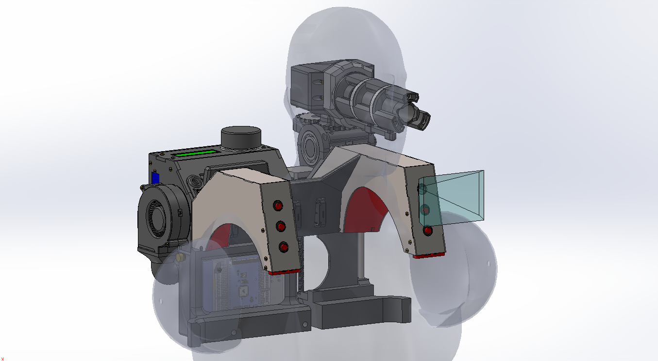
B.A.K.I. (Breakthrough Automated [K]annon Instrument) is my attempt at creating an automated, computer vision Nerf shoulder cannon to fight my younger brothers with.
It consists of a shoulder mount to which a backpack and cannon unit are attached to.
The backpack houses the controls electronics and feeds ammo to the cannon, which can orient itself in 3 DOF (degrees of freedom) to target you 😳


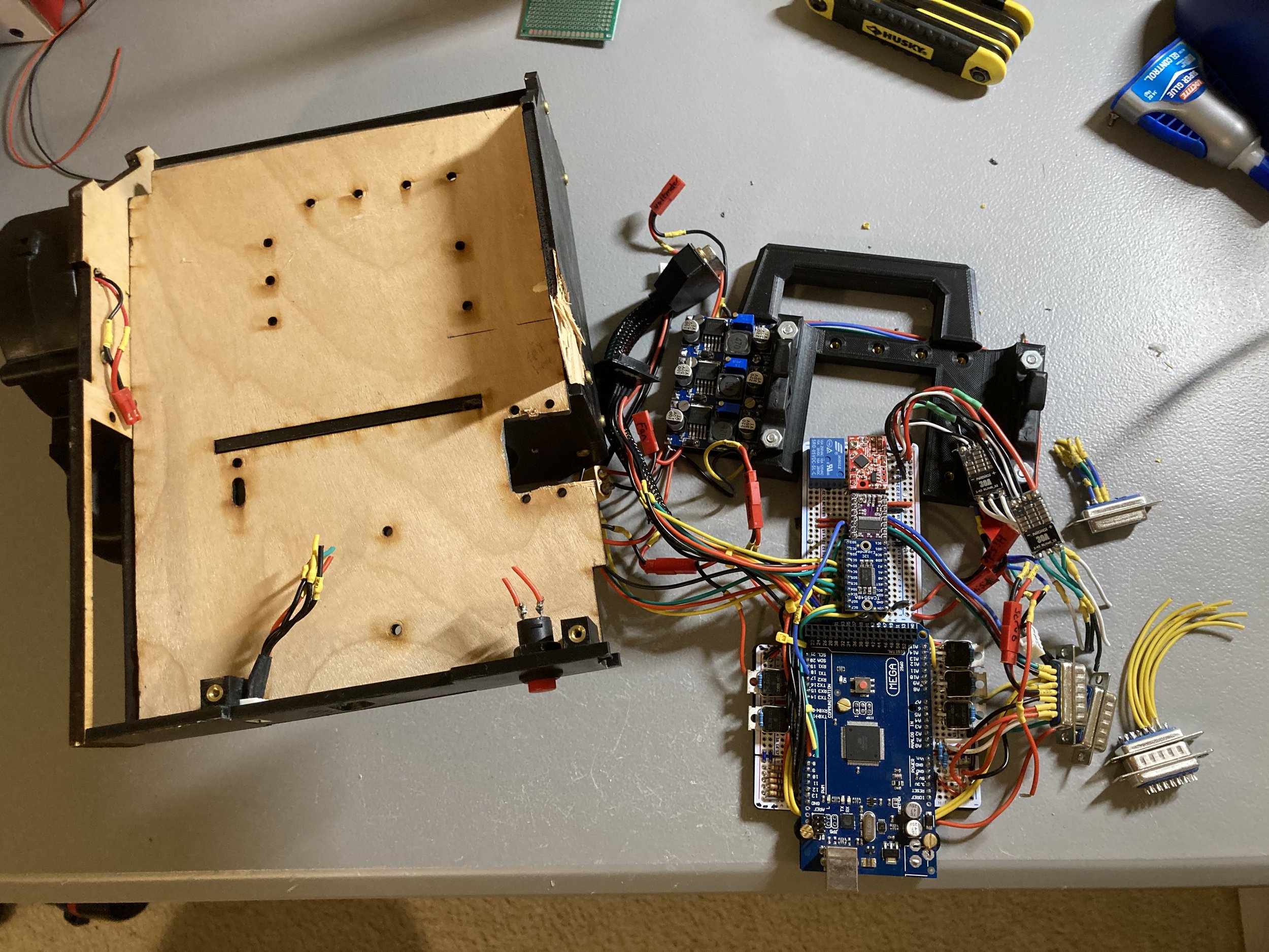
While I got BAKI to a physically 100% complete state, during one of the last stages of testing, I realized the protoboard and components I had used in my hand-wired electronics loom didn’t allow enough current through to fully power the cannon, meaning it would power down, force reset, and repeat.
I had done some power calculations beforehand, and while I realized a printed circuit board (PCB) with high current traces would probably be best, I didn’t know how to make one, and so hand-wired everything, hoping I could get away with just the skills I had at the moment.
However, after testing, I recognized that there was no way around it. The trace thickness in commercially-available protoboards would never be enough for BAKI’s needs (~84 amps when all 9 motors are stalled)
Facing the fact that I’d have to redo the entire electrical with higher current-carrying components, I cut the loom out of the backpack unit. F’s in the chat boyes 😢

While I had initially avoided PCB design to not delay the project in running off to learn a new skill,
I decided that with the project now delayed either way, and having a high-current PCB realistically being the only way forward, I’d do it.
Conveniently, one of my powerlifting buddies, Fredy, was an electrical engineer, and he helped me learn the PCB design software EAGLE!
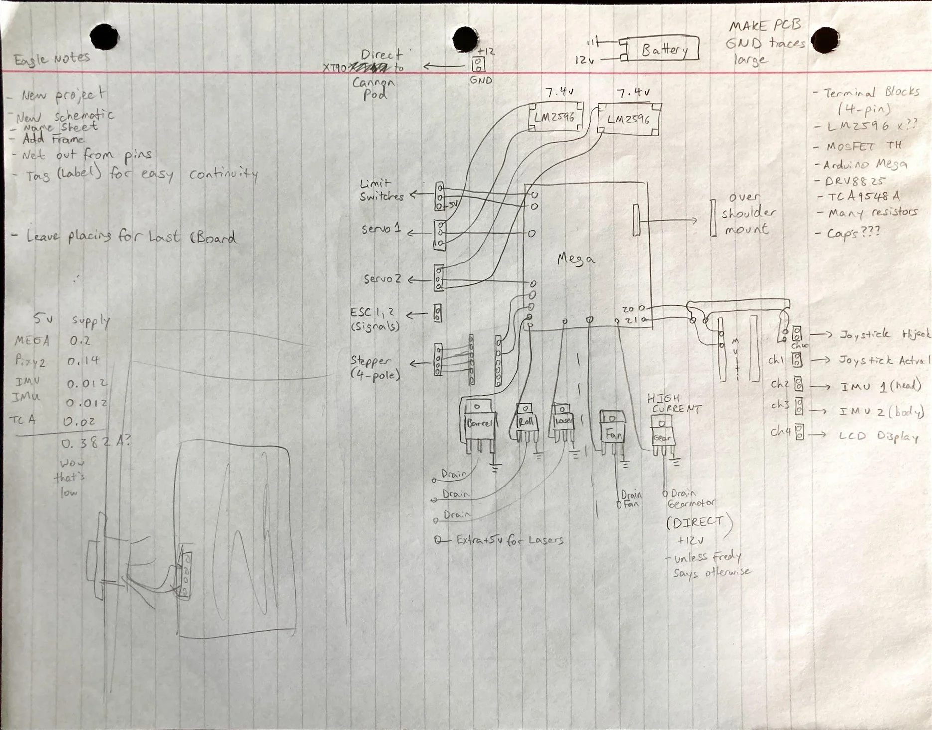

Because I had already made the circuit once by hand, it was easy to redraw it from scratch in an EAGLE-friendly format
From my pencil sketch, I transferred all the elements into EAGLE Schematic, one of two main workspaces within the software
In Schematic, you are just assigning connections between different pins. Just detailing Point A’s and Point B’s, without worrying about the paths between them yet.

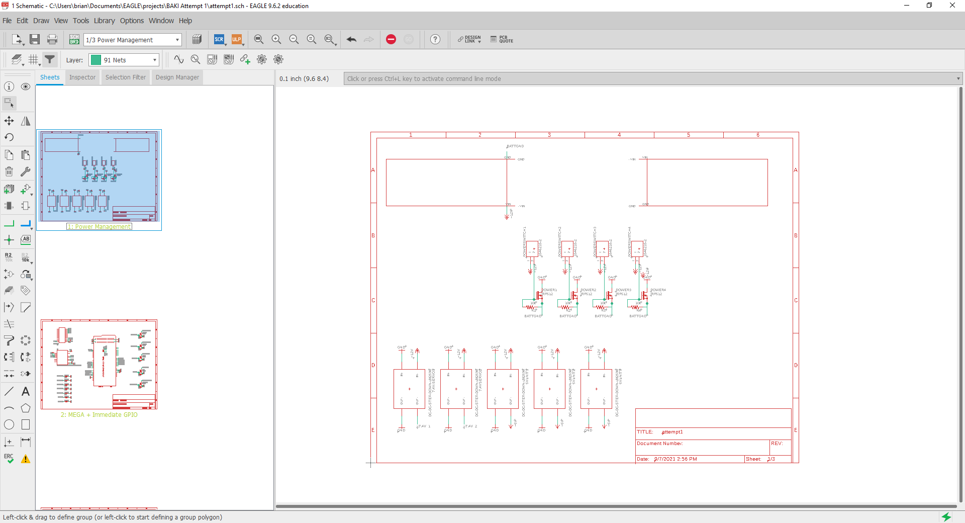
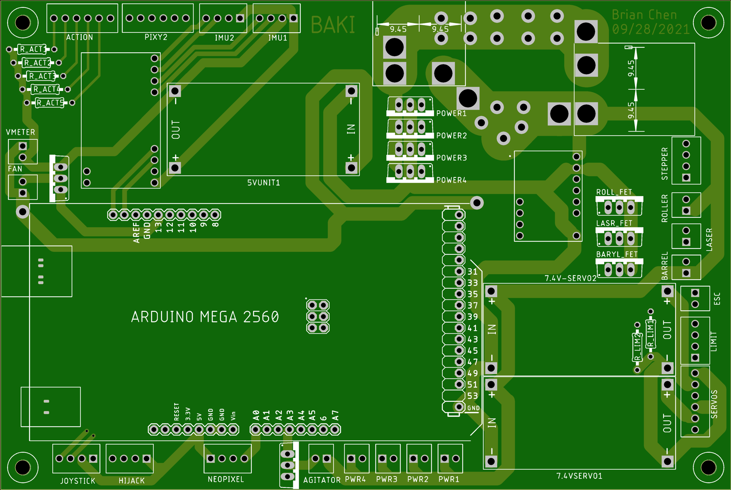
The other workspace, Board, is where you plan the physical placement of your electrical components on the fiberglass PCB body.
(1) My process was to first inventory all of the electronics I needed,
(2) Plan out the spacings in CAD to see what the biggest board I could fit in the backpack was,
(3) then come back and place the electronics footprints in their respective homes in Board

The next step within Board is to route your traces - basically playing connect the dots with copper connections, where the dots are all the Points A and B you set earlier in Schematic. This goes without saying, but the having copper between nodes is what actually lets electricity to conduct through them.
EAGLE has an Autorouter that more often than not gives you suboptimal wirepaths, but it does lend for some cool aesthetic gifs!
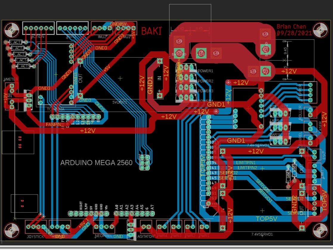
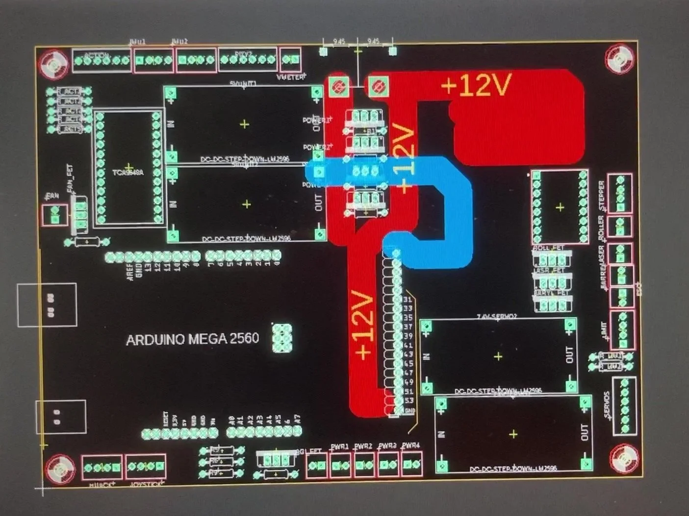
It took a while, but I routed all of my wires by hand, leaving the traces nice and thick for lots of current to flow through.
Some of my traces were 13mm thick (for those without context, that’s a lot!) The red lines represent copper on the PCB’s top face, and blue represents copper on the board’s bottom face.
I had this design looked over by a few Elec friends (thanks Rachel, James, Fasai, & Fredy!! 🥰), before sending it off to the JLCPCB factory for manufacturing.

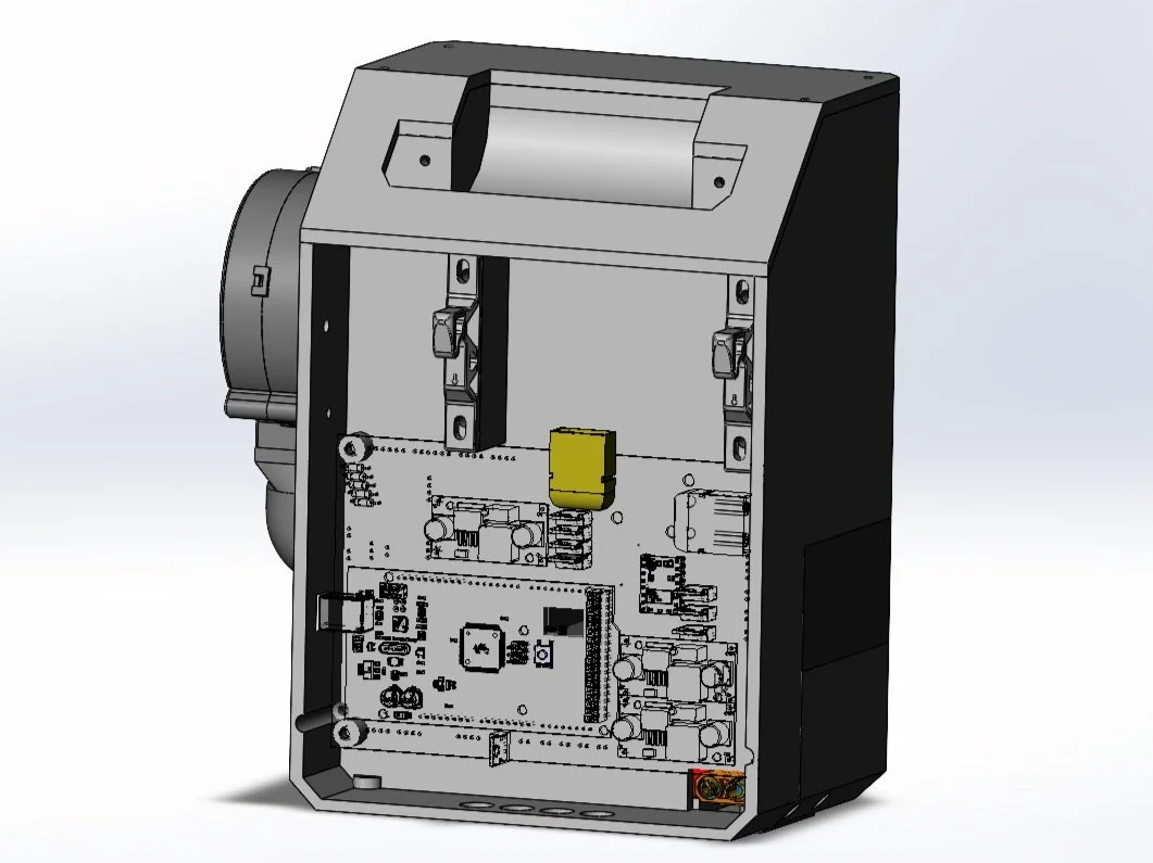
In the meantime, I spent way too much time making a 3D model of my board. I was obsessed
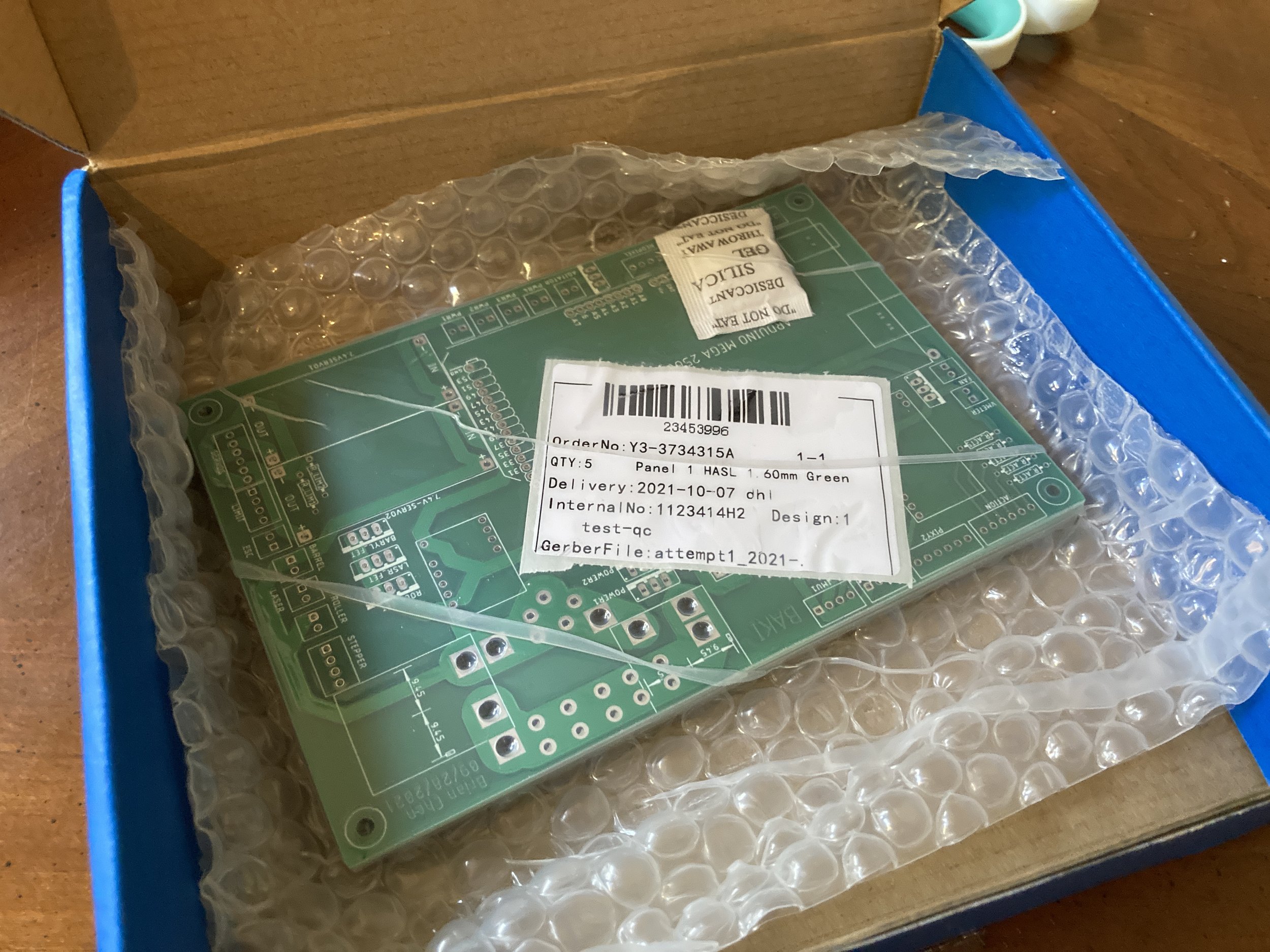


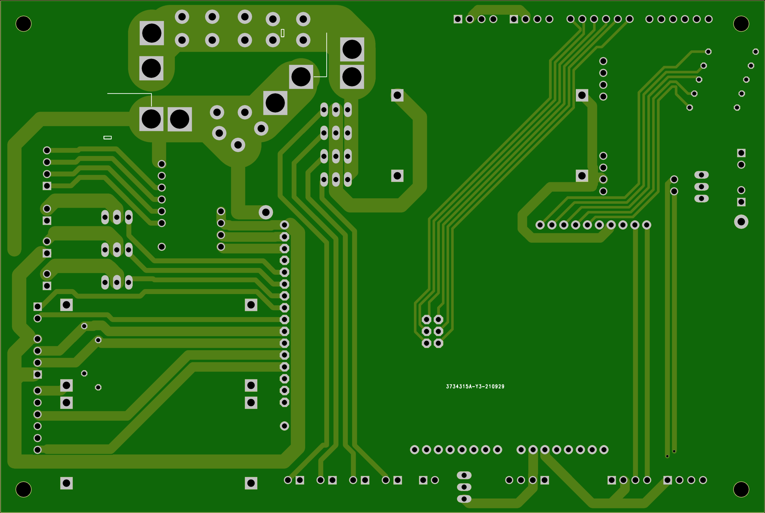
One week-ish later, my PCB blanks arrived! WHOAAAAA!!!!!!!
It was honestly super cool to open the box and see a design I’d spent weeks on, come back in fresh green fiberglass. I think because I typically fabricate all my parts by myself, seeing their every step means there is no surprise at the end. But because these were boards someone else made for me, it was like opening a present 🎁🧧 and really made my day!
(I also wrote my name and the BAKI project name on the board, also super satisfying to see 😎)

I sat down, plugged in all of my electronics, and soldered them in. This took a few hours as opposed to a few days with my handmade board, so I was very thankful. In addition to ability to add high current tracing, PCBs are also much better for high volume / mass production 🤔
It looks so legit! And when I power tested it, everything worked, meaning that I had designed in EAGLE correctly.


Here is the old board v.s. the new — what an improvement! Fredy told me that it’s actually super impressive that I got PCB design right on my first try, so I got a bit full of myself and made the Vegeta meme on the right 🤣
one final effort
And that’s about the current state of the BAKI shoulder cannon! There is just a bit of work to do left (install electronics, test, document, etc.) but I’ve put the project on hold temporarily as I try to find a job. Component costs were getting too high for self-funding, and y’know, trying to be a generally responsible adult 😜
If you’d like to support the build, and happen to be an engineering recruiter or manager, well - HINT HINT 👀
Otherwise, I hope you enjoyed! Hopefully you learned something, or recognized some of my anime references. Maybe stick around for when this gets updated/completed, or check out some other projects?
Thank you for reading!!